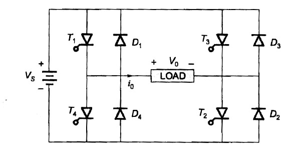
In this article, we will discuss the basics of a Single Phase Full Bridge Inverter such as its working using diagram, waveforms for various loads (R, RL, and RLC ) and in the last the mathematical analysis using the Fourier series. The diagram of a typical single phase full bridge inverter is given below:
Diode 

These Diodes are called Feedback diodes since they conduct only when the Power flow is negative means Power is being fed back to the DC source, when these diodes conduct.
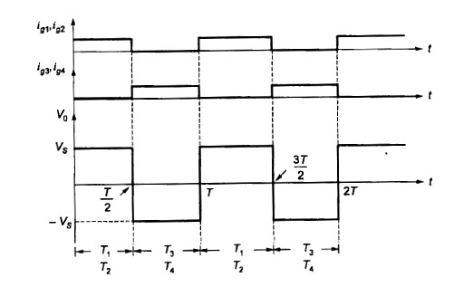
For a Full Bridge Inverter, when 


Steady State Analysis
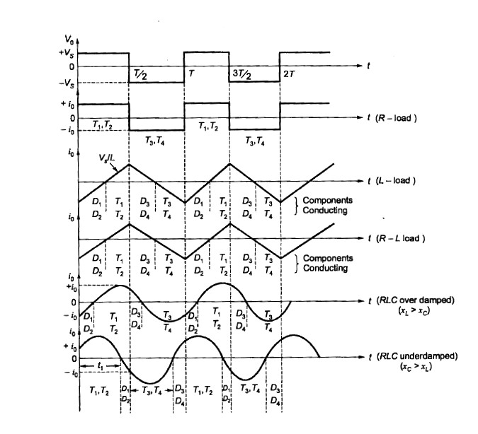
Resistive Load


Each Switching device conducts for 
Each feedback diode conducts for

Pure Inductive Load


Each Switching device conducts for 

Each feedback diode conducts for


RL load
RLC Load
When

Overdamped Response

Characteristcs equation of an 2nd order series RLC System


Forced Commutation is required because to turn OFF the switches 

When

Underdamped Response


Forced Commutation is not required because to turn OFF the switches 
Load Commutation Occurs due to Underdamped Response
![\displaystyle V_{0(\text {rms})} = \left[ \dfrac {1}{T}\; \left( \int_{0}^{\frac {T}{2}} \; V^2_s \; \text {dt} + \int_{\dfrac {T}{2}}^{T} \; V^2_s \; \text {dt} \right) \right]^{\dfrac {1}{2}}](https://s0.wp.com/latex.php?latex=%5Cdisplaystyle+V_%7B0%28%5Ctext+%7Brms%7D%29%7D+%3D+%5Cleft%5B+%5Cdfrac+%7B1%7D%7BT%7D%5C%3B+%5Cleft%28+%5Cint_%7B0%7D%5E%7B%5Cfrac+%7BT%7D%7B2%7D%7D+%5C%3B+V%5E2_s+%5C%3B+%5Ctext+%7Bdt%7D+%2B+%5Cint_%7B%5Cdfrac+%7BT%7D%7B2%7D%7D%5E%7BT%7D+%5C%3B+V%5E2_s+%5C%3B+%5Ctext+%7Bdt%7D+%5Cright%29+%5Cright%5D%5E%7B%5Cdfrac+%7B1%7D%7B2%7D%7D++&bg=ffffff&fg=222222&s=1&c=20201002)

Or
![\displaystyle V_{0(\text {rms})} = \left[ \dfrac {1}{T} \; \left( V^2_{s} \; \times \dfrac {T}{2} + V^2_{s} \; \times \dfrac {T}{2} \right) \right]^{\dfrac {1}{2}} = V_s](https://s0.wp.com/latex.php?latex=%5Cdisplaystyle+V_%7B0%28%5Ctext+%7Brms%7D%29%7D+%3D+%5Cleft%5B+%5Cdfrac+%7B1%7D%7BT%7D+%5C%3B+%5Cleft%28+V%5E2_%7Bs%7D+%5C%3B+%5Ctimes+%5Cdfrac+%7BT%7D%7B2%7D+%2B+V%5E2_%7Bs%7D+%5C%3B+%5Ctimes+%5Cdfrac+%7BT%7D%7B2%7D+%5Cright%29+%5Cright%5D%5E%7B%5Cdfrac+%7B1%7D%7B2%7D%7D+%3D+V_s++&bg=ffffff&fg=222222&s=1&c=20201002)
Output Voltage waveform is Half Wave Symmetric hence all even harmonics are absent

⇒

⇒

![\displaystyle Z_{n} = \left[ R^2 + \left( n \omega L - \dfrac {1}{n \omega C} \right)^2 \right]^{\dfrac {1}{2}}](https://s0.wp.com/latex.php?latex=%5Cdisplaystyle+Z_%7Bn%7D+%3D+%5Cleft%5B+R%5E2+%2B+%5Cleft%28+n+%5Comega+L+-+%5Cdfrac+%7B1%7D%7Bn+%5Comega+C%7D+%5Cright%29%5E2+%5Cright%5D%5E%7B%5Cdfrac+%7B1%7D%7B2%7D%7D%26nbsp%3B+&bg=ffffff&fg=222222&s=1&c=20201002)

hi there,
the article is beautiful. i want to know these statements:
1. Due to load it is not possible because current becomes zero after the voltage becomes zero.
2. Due to load it is possible because current becomes zero before the voltage becomes zero.
my question is how we can arrive at this conclusion from damping ratio. i want to understand the concept. for your kind information, i have studied rlc series ckt.
LikeLike
Hello Gourab
Thanks for the compliment, Nice to hear from you.
For your answer please check the below link –
https://electricalbaba.com/load-commutation/
LikeLike
tanks for your reply
but my question is different. i want to know:
how can you say for overdamped system, “current becomes zero after the voltage becomes zero.”
i specificall want to know this………….
LikeLike
Hi there,
I am stuck. Iam waiting for your assistance
LikeLike
❣️
LikeLike